
Fabrication and characterization of [0001]-oriented Zn metallic electrodes
Determine 1a illustrates a hexagonal closed-packed construction of Zn unit cell, the place the basal floor corresponds to the Zn(0002) aircraft. The Zn(0002) aircraft has a decrease floor vitality of 0.84 J m−2 compared to the Zn((10bar{1}0)) and Zn((10bar{1}1)) planes, confirming its excessive thermodynamic stability29,30. We utilized direct-current electrodeposition in boric acid (H3BO3)/Zn-based options to manufacture Zn metallic electrodes with distinctive crystal morphology on a copper (Cu) foil. This was achieved by way of the incorporation of H3BO3 additive and vigorous stirring, creating a perfect surroundings to eradicate dangerous aspect reactions31,32,33,34,35. Because of this, below the prerequisite of mitigating aspect reactions, the crystallographic orientation and texture of the electrodeposited Zn metals have been solely depending on the anions current within the deposited electrolytes. Detailed experimental parameter regulation is offered in Supplementary Desk 1 and Supplementary Figs. 1–3. The Zn metals deposited from ZnCl2 and Zn(CH3COO)2 methods displayed irregular crystalline orientation, whereas a single (0002)-textured Zn metallic was obtained from the ZnSO4 system, as proven within the scanning electron microscopy (SEM) photos (Fig. 1b–d).
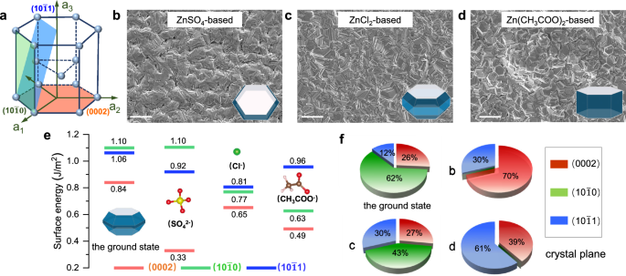
a The illustration of the hexagonal shut packed (hcp) construction of Zn. SEM photos of the electrodeposited Zn metals in (b) ZnSO4, (c) ZnCl2, and (d) Zn(CH3COO)2 methods, respectively (scale bar, 20 μm). The inset photos correspond to the equilibrium form of Zn crystals in several system, obtained from HSE06 calculations. e Floor energies of Cl−, SO42− and CH3COOH− on Zn((10bar{1}0)), Zn((10bar{1}1)) and Zn(0002) planes, respectively. Colours for various atoms: white for H, brown for C, crimson for O, yellow for S and inexperienced for Cl. f The ratios of various crystal planes (Zn((10bar{1}0)), Zn((10bar{1}1)) and Zn(0002)) within the floor state and the electrodeposited Zn crystals of b to c.
To elucidate the function of anions in directing the crystal development of deposited Zn metals, the floor energies (Fig. 1e) of low-index crystal planes (together with Zn((10{bar{1}}0)), Zn((10{bar{1}}1)), and Zn(0002)) have been calculated in these three totally different methods: ZnCl2, ZnSO4, and Zn(CH3COO)2. Selective adsorption of anions resulted in a discount within the floor energies throughout all crystal planes. Notably, the floor vitality of Zn(0002) aircraft within the ZnSO4 system skilled a pointy drop, suggesting a desire for Zn(0002) aircraft publicity within the presence of SO42− anions. Primarily based on the Gibbs-Wulff principle of crystal development, crystals with decrease floor vitality exhibit quicker lateral development charges, consequently rising as the first uncovered crystal planes36. The equilibrium shapes of the ready Zn metals, derived by a Wulff construction37 in these three methods, had totally different crystal morphologies (inset of Fig. 1b–d). Theoretical calculations point out that various the anions of deposited resolution gave rise to crystal texture adjustments (Fig. 1f). Particularly, it’s evident that the ratio of Zn(0002) aircraft within the ZnSO4 system was considerably larger than that in each ZnCl2 and Zn(CH3COO)2 methods, aligning with X-ray diffraction (XRD) patterns (Supplementary Fig. 4).
Contemplating the universality and potential for large-scale utility of the electrodeposited Zn(0002) metallic, we right here used industrial Zn (com-Zn)38 metallic as a management pattern in the entire article. The microstructure of each com-Zn and Zn(0002) metals was systematically investigated by way of XRD, SEM, electron backscatter diffraction (EBSD), and transmission electron microscopy (TEM) observations. In distinction to the one (002) characterised peak of Zn(0002) metallic, the XRD sample (Supplementary Fig. 5) of the com-Zn metallic displayed a number of peaks, implying a disordered crystalline orientation. Moreover, the residual stresses of Zn(0002) metallic (14.8 MPa) have been discovered to be decrease than that of com-Zn metallic (22.8 MPa), indicating minimal lattice pressure and misfit dislocations9,39. Moreover, the com-Zn metallic demonstrated a random and irregular distribution of crystal grains with a mean grain dimension worth of 25.58 ± 0.55 µm (Fig. 2a and Supplementary Fig. 6a), which was additional confirmed by the EBSD characterization (Fig. second and Supplementary Fig. 7a). Conversely, the Zn(0002) metallic confirmed quite a few equiaxed grains with a mean grain dimension of 1.51 ± 0.60 µm (Fig. 2b and Supplementary Fig. 6b, c). The aircraft view EBSD maps and pole figures (Fig. 2e and Supplementary Fig. 7b) revealed that the Zn(0002) metallic introduced a single <0001> texture, displaying a locked crystalline orientation. This consequence was additional demonstrated by TEM (Fig. 2f), quick fourier remodel (FFT), and chosen space electron diffraction (SAED) characterizations. The diffraction spots of the Zn atoms completely matched with the Zn(0002) lattice aircraft and the grain was within the [0001] orientation (Fig. 2h, i), the place the corresponding interplanar spacing of 0.2334 nm was decided to the ((01bar{1}0)) aircraft of Zn40 (Fig. 2g). These complete characterizations of the crystal construction correctly point out that the electrodeposited Zn(0002) metallic has just one [0001]-crystallographic axis.
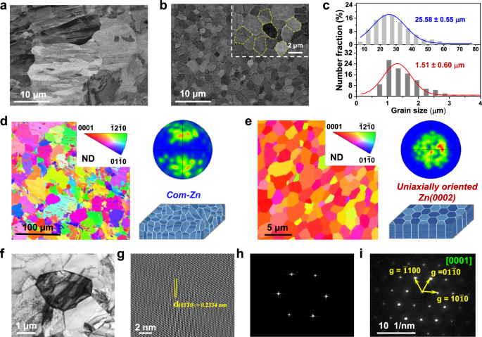
SEM photos of (a) the com-Zn and (b) electrodeposited Zn(0002) metals with an magnified picture of hexagonal Zn grains (inset). c Grain dimension distributions from statistical SEM measurements for the com-Zn and the electrodeposited Zn(0002) metals. 3D illustration, plane-view EBSD maps and corresponding (0002) pole figures of (d) the com-Zn and (e) electrodeposited Zn(0002) metals. Detailed crystallographic statement of the electrodeposited Zn(0002) metallic: f Typical bright-field TEM picture, g corresponding high-resolution TEM picture, h FFT sample and that i 4D-STEM nanobeam diffraction sample of f.
Ex situ morphological and structural evolution of Zn plating/stripping
Zn metallic exhibits a desire for forming disordered and nonplanar platelet electrodeposits at liquid-solid interfaces because of its decrease thermodynamic free energy41,42,43,44,45. The Zn plating course of might be divided into two phases: nucleation and steady development, that are influenced by the present density in accordance with the Bulter-Volmer electrode kinetics relationship46. Notably, the Zn(0002) metallic displayed a decrease nucleation overpotential (ηn) than that of com-Zn metallic, regardless of present density, whereas the plateau overpotential (ηp) exhibited the alternative development (Supplementary Fig. 8a, b). This consequence means that Zn(0002) metallic can suppress dendrite development successfully compared with com-Zn metal47.
In addition to, to analyze the importance of a Zn metallic electrode possessing a single (0002) texture for sustaining epitaxial development, we constructed Zn metallic electrodes with a predominant (0002) texture and a minor presence of different Zn textures as an intermediate state (IMS-Zn(0002)) between com-Zn and single (0002)-textured Zn electrodes. The IMS-Zn(0002) metallic electrode, that includes a mean grain dimension worth of 8.40 ± 0.30 µm, confirmed a hexagonal morphology just like that of the Zn(0002) metallic electrode (Supplementary Fig. 9a and Supplementary Fig. 10a, b). The XRD sample (Supplementary Fig. 9b) of the IMS-Zn(0002) electrode displayed a extremely pronounced (002) peak and a weak (101) peak. The relative texture coefficient (RTC) of every lattice aircraft was calculated utilizing the next formula48,
$$,{{RTC}}_{left({hkl}proper)}=frac{{I}_{({hkl})}/{bar{I}}_{({hkl})}}{sum [{I}_{left({hkl}right)}/{bar{I}}_{left({hkl}right)}]}instances 100$$
(1)
The place, ({I}_{({hkl})}) represents the depth obtained from textured Zn pattern, and ({bar{I}}_{({hkl})}) is the depth of the usual oriented Zn pattern (from JCPDS knowledge). The corresponding RTC(002) of com-Zn, IMS-Zn(0002) and Zn(0002) electrodes was 41, 93 and 100, respectively (Supplementary Fig. 11). This consequence signifies that the IMS-Zn(0002) metallic electrodes had solely a minor ((10bar{1}1)) texture predominantly that includes the (0002) texture, which was additional confirmed by the EBSD characterization (Supplementary Fig. 12a–d).
The morphology evolution of com-Zn, IMS-Zn(0002) and Zn(0002) metallic electrodes throughout plating and stripping was characterised by a collection of in situ and ex situ checks. On the stripping aspect, each com-Zn and IMS-Zn(0002) electrodes exhibited quite a few randomly-sized pores, which turned extra pronounced with discharge time (Supplementary Fig. 13a, b). Corrosion by-products have been even shaped on the com-Zn floor. In distinction, the Zn(0002) floor displayed higher corrosion resistance and a extra ordered stripping course of (Supplementary Fig. 13c). On the plating aspect, scattered and unfastened Zn deposits have been noticed on the com-Zn floor, which quickly grew alongside the separator route (Fig. 3a). The IMS-Zn(0002) electrode maintained a comparatively flat deposition floor in the course of the 10 min plating. Nevertheless, with a rise in deposition time, disordered and uneven Zn deposits shaped on the IMS-Zn(0002) floor (Fig. 3c). In distinction, hexagonal-Zn deposition unfold parallelly with out Zn dendrites on the Zn(0002) floor throughout plating (Fig. 3e). This phenomenon was additional affirmed by way of in situ optical microscopic evaluation in clear Zn||Zn symmetrical cells (Supplementary Fig. 14a, b). Even after 1 h plating, flat and densely packed Zn deposition was noticed on the Zn(0002) floor utilizing confocal laser microscope (LSM, Supplementary Fig. 15a–c), with a decrease floor roughness (0.3 μm) than on com-Zn (2.8 μm) and IMS-Zn(0002) (1.9 μm) surfaces. Ex situ XRD was carried out to detect the structural evolution of Zn metallic electrodes in the course of the charging course of, as proven in Fig. 3b, d, f and Supplementary Fig. 16a–c. The peaks positioned at roughly 36o in each electrodes have been assigned to the (0002) aircraft of Zn crystal49. The XRD patterns confirmed that the deposited Zn on com-Zn and IMS-Zn(0002) surfaces lacked a hard and fast orientation, whereas a single (002) peak was constantly noticed utilizing the Zn(0002) electrode from the start to the tip, illustrating ultra-sustainable epitaxial development between the overgrowth and the substrate crystals. Moreover, there was a major enhance in residual stress for each IMS-Zn(0002) (from 16.5 MPa to 60.8 MPa) and com-Zn (from 22.8 MPa to 110.7 MPa) metallic electrodes earlier than and after deposition 1 h below a present density of 4 mA cm−2. In distinction, the stress of Zn(0002) metallic electrode modified barely from 14.8 MPa to fifteen.7 MPa, indicating negligible lattice pressure and mismatch dislocations of deposited Zn. These findings counsel that whereas using a Zn metallic electrode with a predominant (0002) texture promotes uniform Zn deposition on the preliminary stage, the subsequently deposited Zn exhibits irregular and random development as soon as the deposited layer surpasses the crucial thickness of homoepitaxial development.
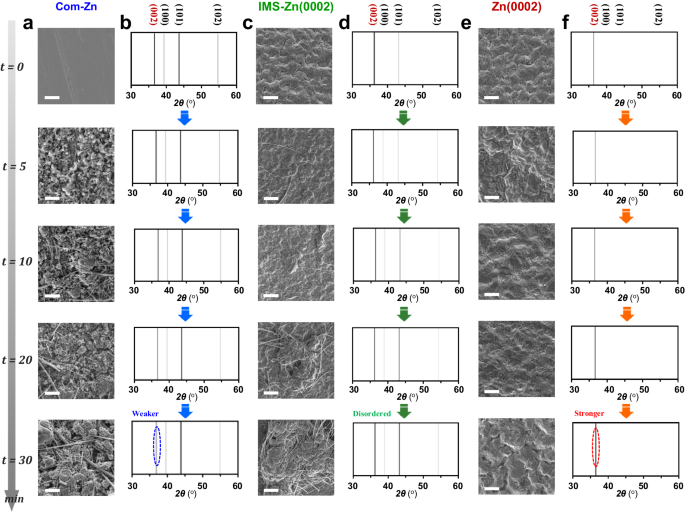
SEM photos of (a) com-Zn, (c) IMS-Zn(0002) and (e) Zn(0002) electrodes in Zn||Zn cells after plating 0 to 30 min (scale bar, 20 μm). XRD patterns of (b) com-Zn, (d) IMS-Zn(0002) and (f) Zn(0002) electrodes after plating from 0 to 30 min. Present density, J = 4 mA cm−2.
Homoepitaxial mechanism of Zn on Zn(0002) metallic electrode
A tolerance lattice mismatch (f < 18%) between overgrowth crystal and substrate crystal is a key consider attaining epitaxial development; this small lattice mismatch is conducive to minimizing the interfacial vitality of the 2 crystals39. Nevertheless, it needs to be famous that the aforementioned principle is solely relevant to thermodynamically secure states50. In battery methods, significantly at excessive present densities, the Zn development fee is significantly accelerated, leading to a kinetic-dominated course of. Moreover, this principle is relevant to a substrate crystal with a single crystalline orientation (Supplementary Fig. 17a). The presence of even a small quantity of different Zn textures within the Zn(0002) metallic electrode induces dislocation on the epitaxial interface (Supplementary Fig. 17b), inflicting lattice distortion. Past the crucial thickness for epitaxial development, subsequently deposited crystals show a disordered crystalline orientation, indicating the failure of the homoepitaxial mechanism. Subsequently, it’s crucial to make sure the Zn(0002) metallic substrate with a single crystalline orientation to eradicate the lattice mismatch at epitaxial interface and supply uninterrupted driving forces for Zn epitaxial development.
Primarily based on a collection of lattice mismatch calculations, it has been noticed {that a} persistent lattice mismatch exists between the Zn(0002) aircraft and the Zn((10bar{1}0)) and Zn((10bar{1}1)) planes, with magnitudes of 6.67% and 42.29%, respectively, as illustrated in Fig. 4b, c. The electrodeposited Zn(0002) electrode introduced a hexagonal close-packed (hcp) construction (Fig. 4a), through which the Zn(0002) planes have been stacked parallelly within the order of “~ABABAB~” mode51, displaying a single Zn(0002) texture, as depicted in Fig. 4d. To conclusively make clear the pivotal function of the substrate crystal that includes a single-Zn(0002) crystalline orientation in figuring out the expansion route of Zn, a nano-beam electron diffraction (NBED) approach was employed in transmission electron microscopy to analyze the underlying epitaxial mechanism within the Zn(0002) metallic. On this regard, TEM foils of the metallic have been sliced from the deposited Zn to the epitaxial interface alongside the route perpendicular to the epitaxial substrate through centered ion beam expertise. We noticed sharp interfaces between the Zn(0002) substrate and the Zn deposits from cross-sectional TEM observations (Fig. 4e). A number of grains (G1, G2, G3, and G4) of the overgrowth crystal have been randomly chosen to characterize its development route utilizing electron diffraction evaluation below TEM, as proven in Fig. 4f, g. The diffraction spots revealed that the lattice of the grains had the very same lattice orientation. Zooming in on nanograins of the deposited Zn below high-resolution TEM, we noticed that the Zn atoms derived from the Zn deposits have been completely matched with the Zn(0002) substrate crystal by the order of “~ABABAB~” association (Fig. 4h). As introduced within the illustration of Fig. 4i, the such Zn(0002) metallic was assumed to allow an epitaxial, relatively than a dendritic, development of Zn to maintain the consistency of the substrate texture. Consequently, Zn metals with a single (0002)-textured crystallographic function allow ultra-sustainable homoepitaxial development.
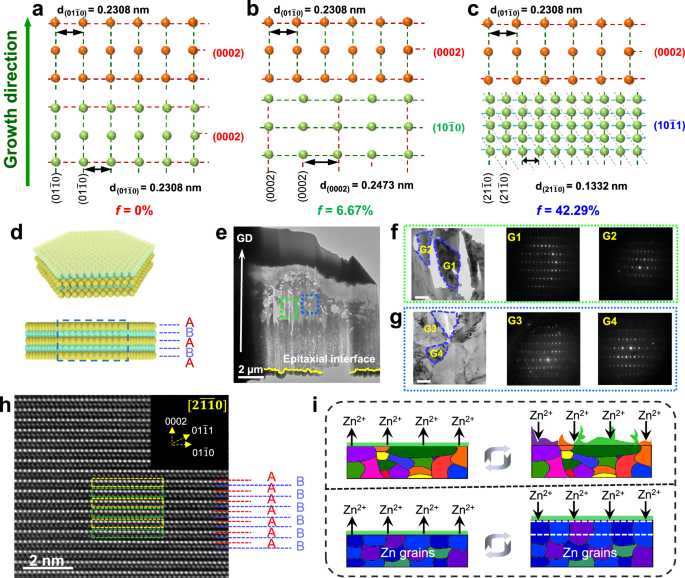
a–c The lattice mismatch of Zn(0002), Zn((10bar{1}0)) and Zn((10bar{1}1)) to Zn(0002), respectively. d The structural illustration of the atomic association of the hexagonal Zn nanosheet. e Typical cross-section TEM picture of the deposited Zn on the Zn(0002) floor alongside development route. The field outlines the world magnified in f, g. f, g Magnified TEM picture of the deposited Zn and the NBED patterns of the chosen Zn grains (scale bar, 200 nm). h The high-resolution TEM picture of the deposited Zn. The NBED sample of element of deposited Zn (inset). i Schematic illustration of the Zn stripping/plating on the floor of com-Zn and Zn(0002) electrodes.
Electrochemical efficiency of Zn metallic electrodes
To precisely assess the reversibility of Zn metallic electrodes, their CE have to be quantified in Cu||Zn half cells. Cu||com-Zn cells exhibited failure after solely 97 cycles at 1 mA cm−2/1 mAh cm−2, whereas Cu||Zn(0002) cells displayed a powerful common CE of 99.6% over 330 cycles (Supplementary Fig. 18a). Even at a big present density and capability of 5 mA cm−2 and 5 mAh cm−2, the Zn(0002) electrode may stably cycle for 220 cycles, with a excessive common CE of 99.5% because of its superior corrosion resistance of Zn(0002) electrode (Supplementary Fig. 18b). The longevity and voltage polarization of Zn||Zn symmetric cells have been additional analyzed, the place Zn||Zn cells comprising Zn(0002) electrodes demonstrated an extended cycle life and decrease voltage polarization than these with com-Zn electrodes (Supplementary Fig. 19a–c). Moreover, the speed efficiency of Zn||Zn cells with Zn(0002) electrodes surpassed these with com-Zn electrodes, confirming the excessive reversibility of the Zn(0002) metallic electrode (Supplementary Fig. 20)52. A half-cell experiment was carried out on Zn electrodes with a 3-electrode configuration to calculate the hydrogen evolution response (HER) fee by linear sweep voltammetry (LSV) curves53,54. It’s evident that the HER of the Zn(0002) electrode occurred at a extra unfavorable potential than that of com-Zn electrode (Supplementary Fig. 21a, b). These outcomes exhibit that the one (0002)-textured Zn metallic electrode can successfully inhibit HER compared with com-Zn, attributed to the superior thermodynamic stability of the Zn(0002) crystal aircraft. Moreover, XRD, X-ray photoelectron spectroscopy (XPS) and electron probe microanalysis (EPMA) have been employed to additional examine their corrosion habits. As proven in Supplementary Fig. 22, the brand new peak on com-Zn at round 8.25o, recognized to Zn4SO4(OH)6·5H2O (ZHS) by-products55, was considerably lowered on Zn(0002), suggesting its corrosion resistance impact. This consequence was in step with the XPS spectra and EPMA wavelength-dispersive X-ray spectroscopy (WDS) photos of the cycled Zn electrode, as depicted in Supplementary Figs. 23a, b and 24a, b. Contemplating the outstanding enhance within the nucleation and development fee of Zn at massive currents, the soundness of the Zn||Zn cells below 75.2% DODZn was examined utilizing skinny Zn metallic electrodes (45 μm, 26.3 mAh cm−2). The outcomes introduced in Fig. 5b, c demonstrated that the corresponding Zn||Zn cells with Zn(0002) electrodes can stably cycle for over 250 h, whereas these with com-Zn electrodes have been short-circuited after 51 h. Subsequently, the Zn(0002) metallic electrode has important potential for sensible functions to acquire improved efficiency and longer lifespans.
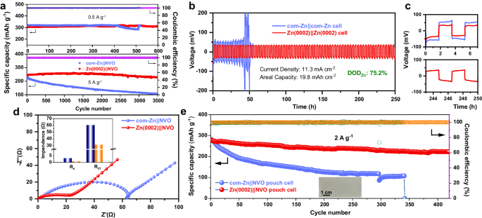
a Cyclic functionality of the Zn||NVO coin cells utilizing com-Zn and Zn(0002) anodes at totally different present densities (0.5 A g−1 and 5 A g−1). b Biking efficiency of the Zn||Zn cells with a restricted Zn provide (DODZn = 75.2%), a present density of 11.3 mA cm−2, and a areal capability of 19.8 mAh cm−2. c The chosen enlarged voltage profiles of b. d Electrochemical impedance spectra curves of the com-Zn||NVO and the Zn(0002)||NVO cells. The inset exhibits associated dependence of Rs and Rct. e Biking efficiency of the Zn||NVO pouch cell utilizing com-Zn and electrodeposited Zn(0002) anodes. The areal capability of pouch cells is ~2 mAh cm−2.
The Zn metallic electrodes have been additionally examined in full cells configuration utilizing a NH4V4O10 (NVO) cathode and three M ZnSO4 electrolyte. The com-Zn||NVO cells exhibited speedy capability decay, whereas the Zn(0002)||NVO cells delivered biking stability of as much as 600 and 3500 cycles with a capability retention of as much as 98% at 0.5 A g−1 and 5 A g−1, respectively (Fig. 5a). The normalized discharge/cost profiles of the Zn||NVO cells revealed that the com-Zn||NVO cell had a higher voltage hysteresis than the Zn(0002)||NVO cell (Supplementary Fig. 25). The preliminary cells of Zn||NVO have been characterised by a Nyquist plot to allow the extrapolation of the cost switch resistance (Rct). The EIS knowledge (Fig. 5d) indicated that the Rct of the Zn(0002)||NVO cell (31.35 Ω) was considerably lower than that of the com-Zn||NVO cell (60.37 Ω), suggesting that Zn(0002) anode facilitated cost switch kinetics56. Even after 1000 cycles, the Zn(0002)||NVO cell nonetheless delivered a considerably lowered Rct than that of the com-Zn||NVO cell, indicating that the Zn(0002) held promise in regulating Zn epitaxial development and suppressing aspect reactions (Supplementary Fig. 26). In addition to, the decrease Rct of Zn(0002) in comparison with that of com-Zn was attributed to its larger change present density (({i}_{0})) (Supplementary Fig. 27), indicating the quick deposition kinetic of the Zn(0002) electrode. The Zn(0002)|| NVO cell exhibited larger particular capacities than these with com-Zn anode at particular present of 1, 2, 5, 10, and 20 A g−1 (Supplementary Fig. 28a–c). This consequence was supported by the cyclic voltammetry (CV) response of the complete cell at a scan fee of 1 mV s−1 (Supplementary Fig. 29). The SEM photos of Supplementary Fig. 30 demonstrated that, in distinction to the com-Zn anode, the Zn(0002) grains remained totally intact even after 1000 cycles, strongly indicating the ultra-sustainable epitaxial development of Zn(0002) metallic throughout biking. Biking checks of Zn||NVO pouch cells have been carried out in Fig. 5e, and the capability retention of Zn(0002)||NVO pouch cells was 80% after 450 cycles however that of com-Zn||NVO pouch cells was solely 61% after 100 cycles and confirmed unstable CEs. Moreover, Zn(0002)||NVO pouch cells generated a secure present that illuminated a lightweight and rotated a fan (Supplementary Fig. 31a, b; Supplementary Film 1, 2).


